

Otras habilidades populares


Trabajos destacados
Explora nuestra lista actual de principales proyectos destacados.
Encontrar concursos
Descubre tu talento y encuentra concursos de freelancer en los cuales participar.


Otros trabajos populares
Encuentra trabajos en diferentes idiomas
Empresarial
Potencia tu ventaja competitiva con Freelancer Enterprise.
Servicios de campo
Ofrece tu experiencia en cualquier lugar del mundo a gran escala y bajo demanda.
IA para negocios
Deja que los expertos en lo último en tecnología transformen tu negocio.
Productos de Freelancer
Retos de innovación
Convierte retos en avances con el mayor centro de innovación.
API de Freelancer
Utiliza la API de Freelancer para acceder a una fuerza laboral en la nube de freelancers expertos.
Trabajos locales
Recibe ayuda en cualquier lugar del mundo.
Servicios de freelancers
Cómo funciona

Obtén ideas

Recursos

Ahora estás siguiendo a
Error al seguir a usuario.
Este usuario no permite que los usuarios lo sigan.
Ya estás siguiendo a este usuario.
Tu plan de membresía solo permite 0 seguimientos. Mejora tu membresía aquí.
Dejaste de seguir correctamente a
Error al dejar de seguir al usuario.
Has recomendado exitosamente a
Error al recomendar al usuario.
Algo salió mal. Por favor, actualiza la página e intenta de nuevo.
Email verificado correctamente.
Sikhamani B.
@SIKHAMANI
5,0
1
2,2
2,2
100%
Sr PCB Design Engineer
$20 USD / hora
・

India (3:29 p. m.)
・
Se unió el julio 12, 2016
$20 USD / hora
・
1. Have 13 years of rich experience in PCB Layout, when it comes to PCB design, am capable of developing all kinds of PCB boards independently with complete cycle from scratch to fabrication.
2. High speed PCB layout with Altium Layout Tools.
3. Have experience in delivering PCB CAD layout of High Density – High speed, mixed, Analog, Digital, RF designs, flex designs etc.
4. Worked on many high-speed interfaces like Thunderbolt Type-C, PCIE-Gen4, LPDDR5, eDP, CSI, HDMI, and USB3 in INTEL SoCs.
5. Have experience in HDI Micro via technology, Multilayer PCB Layout & routing, impedance/length matching, RF design, blind/buried vias.
6. Have experience in setting constraints for DFA, DFM, DFT and interface design class and types.
7. Have knowledge of Signal integrity, RF, Power integrity, EMI/EMC, Mechanical and Thermal analysis with respect to PCB board layout.
8. Capable of working long hours.
Verificaciones
A tiempo
100 %
Dentro del presupuesto
100 %
Aceptar tarifa
100 %
Portafolio
Portafolio

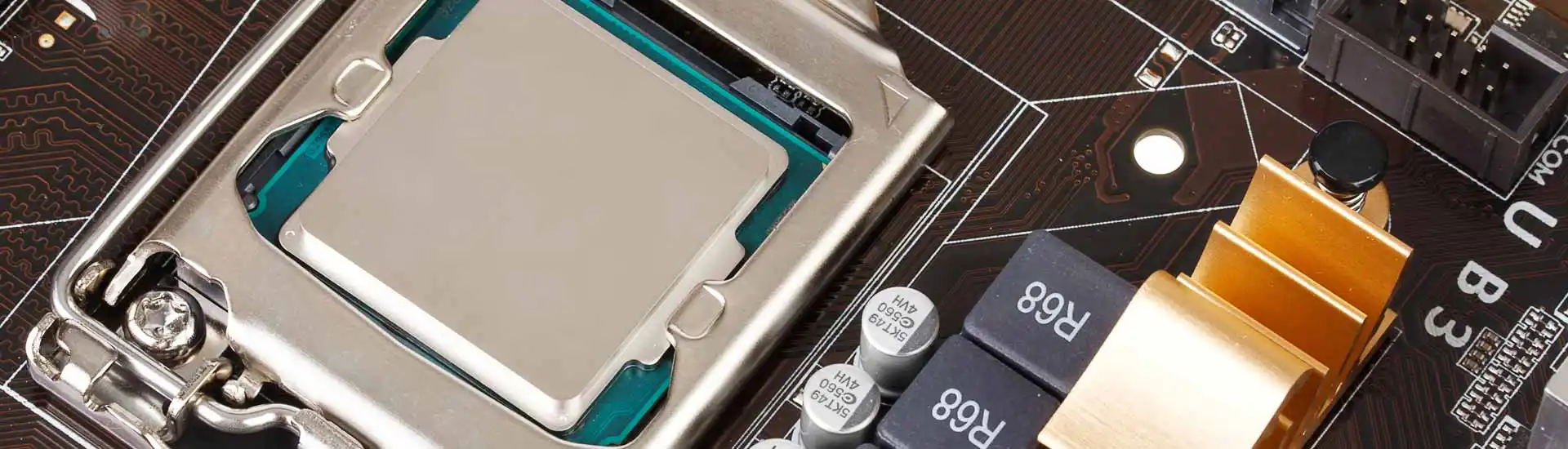
Daughter Board (PCB)

Edge Gold Finger FPGA DDR4

RF FPGA 50GHz
Daughter Board (PCB)
Edge Gold Finger FPGA DDR4
RF FPGA 50GHz
Cambios guardados
Sikhamani has good knowledge and he works hard and focused for his task for best results. I will prefer to work with him again.
Aditya Singh P.
@parmaraditya4497
•
Ahmedabad, India
•
Compartir
Experiencia
Sr PCB Design Engineer
ago, 2022 - Presente
•
2 años, 5 meses
Freelancer
ago, 2022 - Presente
•
2 años, 5 meses
1. Schedule & Design planning
2. Get all required details from client
3. Import/Export netlist and interact with DEs and Mechanical team for Layout implementation
4. Multi-layers upto32 Layers PCB designing, constraints settings.
5. DFM checks using by Valor tool & View mate.
6. Stackup and material design for fabrication.
7. Providing EQs response to FAB vendors.
8. Design reviews done by peers.
ago, 2022 - Presente
•
2 años, 5 meses
Senior VLSI Engineer
mar, 2021 - ago, 2022
•
1 año, 5 meses
Wipro Limited
mar, 2021 - ago, 2022
•
1 año, 5 meses
1. Start with kickoff meeting of new project and Netlist/floorplan/Board outline/Component Placement
2. Set all required design rules in constraint manager & stackup details
3. Assign the task to team members on priority things
4. Syncup with client team for opens/reviews/schedule tracking
5. Identify roadblocks/issues to bring up to team notice and resolve
6. Complete the design without any issues/defects/ reported by client/PCB manufacturer
mar, 2021 - ago, 2022
•
1 año, 5 meses
Educación
Jawaharlal Nehru Technological University
2004 - 2008
•
4 años
B.Tech
India
2004 - 2008
•
4 años
¡Invitación enviada correctamente!
¡Gracias! Te hemos enviado un enlace para reclamar tu crédito gratuito.
Algo salió mal al enviar tu correo electrónico. Por favor, intenta de nuevo.
Freelancer
Información
Términos
Socios
Apps
Falló el copiado al portapapeles. Intenta de nuevo después de ajustar tus permisos.
Copiado al portapapeles.
Cargando visualización previa
Permiso concedido para Geolocalización.
Tu sesión de acceso ha expirado y has sido desconectado. Por favor, inica sesión nuevamente.