Images of paraffin monolayer crystals with perfect contrast: minimization of beam-induced specimen motion
- PMID: 21185452
- PMCID: PMC3741612
- DOI: 10.1016/j.ultramic.2010.10.010
Images of paraffin monolayer crystals with perfect contrast: minimization of beam-induced specimen motion
Abstract
Quantitative analysis of electron microscope images of organic and biological two-dimensional crystals has previously shown that the absolute contrast reached only a fraction of that expected theoretically from the electron diffraction amplitudes. The accepted explanation for this is that irradiation of the specimen causes beam-induced charging or movement, which in turn causes blurring of the image due to image or specimen movement. In this paper, we used three different approaches to try to overcome this image-blurring problem in monolayer crystals of paraffin. Our first approach was to use an extreme form of spotscan imaging, in which a single image was assembled on film by the successive illumination of up to 50,000 spots, each of a diameter of around 7 nm. The second approach was to use the Medipix II detector with its zero-noise readout to assemble a time-sliced series of images of the same area in which each frame from a movie with up to 400 frames had an exposure of only 500 electrons. In the third approach, we simply used a much thicker carbon support film to increase the physical strength and conductivity of the support. Surprisingly, the first two methods involving dose fractionation in space or time produced only partial improvements in contrast whereas the third approach produced many virtually perfect images, where the absolute contrast predicted from the electron diffraction amplitudes was observed in the images. We conclude that it is possible to obtain consistently almost perfect images of beam-sensitive specimens if they are attached to an appropriately strong and conductive support; however great care is needed in practice and the problem remains of how to best image ice-embedded biological structures in the absence of a strong, conductive support film.
Copyright © 2010 Elsevier B.V. All rights reserved.
Figures


bright-field defocused electron diffraction pattern showing paraffin crystal darker than surround due to the diffraction of the primary beam into the diffraction orders. The black square shows the central area used for the high magnification image.
dark-field defocused electron diffraction pattern, showing the six strong spots at 3.7 - 4.1 Å. Each of these dark-field diffraction spots contains about 1.2% of the direct beam intensity at 300keV, causing the crystal in (a) to appear darker than the incident beam, by 6-8% when the crystal is well aligned.
combination of (a) and (b) with contrast modified to show bright-field and dark-field in the same panel. Note that panels (a), (b) and (c) show the same image with different thresholds and gamma values.
spots in the computed diffraction pattern of the high magnification (39,000×) image
power in transforms of selected diffraction spots in the calculated Fourier transforms (diffraction patterns) of images, showing pseudo-dark-field images. Note that the region of the crystal being imaged at high resolution in this case is smaller than the crystal so the whole area is crystalline. These pseudo-dark-field images effectively show which regions of each crystal contribute to the Fourier component that is allowed through the mask, as explained in the last paragraph of section 3.
power from all spots
(2,0)
(1,1)
(1,−1)

spotscan image 011643rmg, using 110 nm diameter spots, with an exposure of 12msec/spot using a 20 μm C2 aperture.
computed diffraction pattern of image and indexing of the main crystal. There are also arc-shaped diffraction spots from a smaller fragment of a different less well-ordered crystal, which partially overlaps with the main crystal and extends into the bottom right corner of the field of view.
pseudo-dark-field image showing power from all three diffraction spots shown in the image and from the individual spots, as in Fig. 2(e). The power in each illuminated spot, recorded sequentially in time, varies between and within the spots across the crystal. The crystal covers the whole area except for a small region in the bottom right corner. The slight Moire pattern visible in the (1,1) panel comes from interference with underlying fragment of the other crystal whose blurry diffraction pattern can be seen in (b).

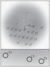
image A16973 showing the raster of spots about 300 μm apart (7-8 nm at 39,000× magnification), recorded with an average exposure of 0.5 el/Å2. The inset shows a smaller area at higher defocus in which the raster is more apparent.
computed diffraction pattern of image. The three paraffin diffraction spots at 3.7-4.1 Å resolution are labeled. The pattern from the hexagonal nanospotscan lattice can also be seen near the origin.
pseudo-dark-field images from all spots, and from the individual (2,0), (1,1) and (1,−1) Fourier components, showing the regions of the image from which the power for each spot comes. The top edge is one edge of the scan raster seen also in (a). The bottom edge is a facet of the crystal. The dark spot is the damaged area in the centre of the scanned area, which was used to adjust the focus before recording the image. The dark and light shadows are regions of CTF minima and maxima, dependent on defocus, crystal tilt (estimated to be less than ±15 nm across the field of view) and beam tilt.

defocused electron diffraction pattern of a crystal viewed on the Medipix II-Quad detector. Some of the pixel defects in the detector including a large damaged area just above the centre can be seen. The 6 diffraction spots at 4Å as well as all the higher resolution spots are clearly visible, showing the sharp outline of the crystal and all areas diffracting well. The central square area has been rendered at a lower level to show the much stronger direct beam and the bright field image of the crystal.
single frame from a 160-frame sequence, with a magnified insert at the top right, showing the individual pixels that have received a single count and the majority of pixels with no counts. Each frame in the series (para_22may_image07) had an exposure of 5000 electrons, corresponding to ~0.006 el/Å2.
transforms added together to show the diffraction spots. The calculation in this case was carried out by summing the 32 power spectra of a 5-frame running average. This was one of the few images that showed spots in all three directions. Others showed two or only one diffraction spot despite the visualization of all three pairs of spots during the initial crystal selection step. The background is much higher when intensities from individual frames are summed, rather than amplitudes being summed as in a single image where the dose has not been fractionated, so the signal-to-noise ratio of the spots is lower. Note that the summing of intensities in this way does not affect the measurement of Ig/I0 and avoids the need to determine the image shifts due to stage drift between frames that builds up over the extended several minute duration of the exposure.

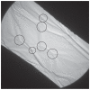
bright-field region in centre of defocused electron diffraction pattern showing the diamond-shaped paraffin crystal A03141. The conditions for recording the images shown in panels (a) to (d) are described in Materials and Methods, paragraph 2.
the same image as in (a) but with much lower threshold to show the dark-field defocused electron diffraction pattern region outside the illuminating beam. Recorded before the high resolution image exposure, it shows the 6 diffraction spots at 3.7 - 4.1 Å resolution with approximately equal intensity.
subsequent dark-field defocused image recorded immediately following the high resolution image exposure. It shows that, at liquid nitrogen temperature after an exposure of 2 el/Å2 at 300keV, well over half of the diffracted intensity remained in the ~4 Å diffracted spots.
final dark-field defocused image recorded after further irradiation with over 20 el/Å2, showing clearly the damage to the irradiated region.
computed diffraction pattern of high magnification image with indexing.
pseudo-dark-field images showing the regions of the image that contribute to each of the three spots at 3.7 - 4.1 Å resolution. The dark and light shadows are regions of CTF minima and maxima, dependent on defocus, crystal tilt (estimated to be less than ±15 nm across the field of view) and beam tilt.


Similar articles
-
Stroboscopic image capture: reducing the dose per frame by a factor of 30 does not prevent beam-induced specimen movement in paraffin.Ultramicroscopy. 2007 Feb-Mar;107(2-3):106-15. doi: 10.1016/j.ultramic.2006.06.005. Epub 2006 Jul 24. Ultramicroscopy. 2007. PMID: 16905258
-
Electron microscopy of biological macromolecules: bridging the gap between what physics allows and what we currently can get.Microsc Microanal. 2004 Feb;10(1):21-7. doi: 10.1017/S1431927604040164. Microsc Microanal. 2004. PMID: 15306063
-
Improved specimen preparation for cryo-electron microscopy using a symmetric carbon sandwich technique.J Struct Biol. 2004 Jun;146(3):325-33. doi: 10.1016/j.jsb.2004.01.012. J Struct Biol. 2004. PMID: 15099574
-
Specimen Behavior in the Electron Beam.Methods Enzymol. 2016;579:19-50. doi: 10.1016/bs.mie.2016.04.010. Epub 2016 May 31. Methods Enzymol. 2016. PMID: 27572722 Review.
-
Processing of Cryo-EM Movie Data.Methods Enzymol. 2016;579:103-24. doi: 10.1016/bs.mie.2016.04.009. Epub 2016 Jun 1. Methods Enzymol. 2016. PMID: 27572725 Review.
Cited by
-
Progress towards an optimal specimen support for electron cryomicroscopy.Curr Opin Struct Biol. 2016 Apr;37:81-9. doi: 10.1016/j.sbi.2015.12.007. Epub 2016 Jan 14. Curr Opin Struct Biol. 2016. PMID: 26774849 Free PMC article. Review.
-
Reaching the information limit in cryo-EM of biological macromolecules: experimental aspects.Biophys J. 2011 May 18;100(10):2331-7. doi: 10.1016/j.bpj.2011.04.018. Biophys J. 2011. PMID: 21575566 Free PMC article. Review.
-
Ultrastable gold substrates: Properties of a support for high-resolution electron cryomicroscopy of biological specimens.J Struct Biol. 2016 Jan;193(1):33-44. doi: 10.1016/j.jsb.2015.11.006. Epub 2015 Nov 22. J Struct Biol. 2016. PMID: 26592474 Free PMC article.
-
Electron counting and beam-induced motion correction enable near-atomic-resolution single-particle cryo-EM.Nat Methods. 2013 Jun;10(6):584-90. doi: 10.1038/nmeth.2472. Epub 2013 May 5. Nat Methods. 2013. PMID: 23644547 Free PMC article.
-
Cryo-EM Grid Preparation of Membrane Protein Samples for Single Particle Analysis.Front Mol Biosci. 2018 Jul 31;5:74. doi: 10.3389/fmolb.2018.00074. eCollection 2018. Front Mol Biosci. 2018. PMID: 30131964 Free PMC article. Review.
References
-
- Hayward SB, Glaeser RM. Radiation damage of purple membrane at low temperature. Ultramicroscopy. 1979;4:201–210. - PubMed
-
- Stark H, Zemlin F, Boettcher C. Electron radiation damage to protein crystals of bacteriorhodopsin at different temperatures. Ultramicroscopy. 1996;63:75–79.
-
- Dubochet J, Adrian M, Chang JJ, Homo JC, Lepault J, McDowell AW, Schultz P. Cryo-electron microscopy of vitrified specimens. Q. Rev. Biophys. 1988;21:129–228. - PubMed
Publication types
MeSH terms
Substances
Grants and funding
LinkOut - more resources
Full Text Sources
Other Literature Sources

