Review
. 2023 Dec 11;18(1):153.
doi: 10.1186/s11671-023-03938-x.

Advances in lithographic techniques for precision nanostructure fabrication in biomedical applications

Affiliations
Review

Advances in lithographic techniques for precision nanostructure fabrication in biomedical applications

Kate Stokes et al. Discov Nano. .

Abstract

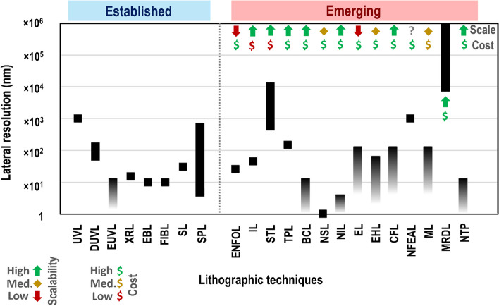
Nano-fabrication techniques have demonstrated their vital importance in technological innovation. However, low-throughput, high-cost and intrinsic resolution limits pose significant restrictions, it is, therefore, paramount to continue improving existing methods as well as developing new techniques to overcome these challenges. This is particularly applicable within the area of biomedical research, which focuses on sensing, increasingly at the point-of-care, as a way to improve patient outcomes. Within this context, this review focuses on the latest advances in the main emerging patterning methods including the two-photon, stereo, electrohydrodynamic, near-field electrospinning-assisted, magneto, magnetorheological drawing, nanoimprint, capillary force, nanosphere, edge, nano transfer printing and block copolymer lithographic technologies for micro- and nanofabrication. Emerging methods enabling structural and chemical nano fabrication are categorised along with prospective chemical and physical patterning techniques. Established lithographic techniques are briefly outlined and the novel lithographic technologies are compared to these, summarising the specific advantages and shortfalls alongside the current lateral resolution limits and the amenability to mass production, evaluated in terms of process scalability and cost. Particular attention is drawn to the potential breakthrough application areas, predominantly within biomedical studies, laying the platform for the tangible paths towards the adoption of alternative developing lithographic technologies or their combination with the established patterning techniques, which depends on the needs of the end-user including, for instance, tolerance of inherent limits, fidelity and reproducibility.


Conflict of interest statement

The authors declare no competing interests.

Figures

Fig. 1
Fig. 1
a(i) Photography of the wafer after deep-UV and dry etching steps. (ii) Single plasmonic chip containing eight plasmonic pixels. (iii) SEM image of the nanohole array with a hole diameter of 200 nm and an array period of 600 nm. b Fabrication steps of the nanohole arrays on free-standing silicon nitride membrane (i–iv). Image from [91]. c Schematic illustration of extreme ultraviolet lithography process. Adopted with permission from [99]. d Diagram of x-ray lithography (adopted with permission from [42]). e Schematic diagram illustrating the evanescent near-field optical lithography (ENFOL) process. Image from [89]
Fig. 2
Fig. 2
a Benefits of immersion lithography. (i) Increased depth-of-focus due to a smaller angle θ in the coupling medium. (ii) Increased resolution with higher numerical aperture optics by coupling light at larger incident angles. Image from [167]; reprinted with permission from [166]. b Two typical implementations of stereolithography for rapid prototyping of ceramics. (i) Top-down system with scanning laser on top and (ii) bottom-up systems with digital light projection. Image from [173]
Fig. 3
Fig. 3
a. Two-photon lithography. Two UV photons react with the photopolymer to produce a pattern. b Block copolymer lithography. A block copolymer and the various structures which can be produced by altering the ratio of monomers. c Nanosphere lithography. Nanobeads are deposited on a substrate and metallised. The nanospheres are then removed to produce the patterned substrate. d UV nanoimprint lithography. The photopolymer fills a stamp and is cured with UV light and the stamp is then removed to produce the final structure. e Phase-shift edge lithography. The photopolymer fills a stamp, and the constructive and destructive interference of light cures areas of the photoresist. The stamp is removed to produce the final pattern. f Electrohydrodynamic lithography. A voltage applied across parallel plates induces instabilities in a polymer film with the possibility of producing various nano geometries. g Capillary force lithography. The polymer is heated and fills the stamp through capillary forces. The polymer is then cured, and the stamp is removed
Fig. 4
Fig. 4
a Preparation of micro-grooved polymeric substrate using near-field electrospinning-assisted lithography (NFEAL). Image from [293]. b Scheme of two approaches using positive and negative magneto-lithography. The magnetic mask installed at the backside of the substrate and the magnet that is set under the mask induce a magnetic field toward the substrate through the pattern of the masks. In the positive approach, the magnetic nanoparticles (NPs) react chemically with the substrate. Hence, the magnetic NPs are immobilized on selective locations, where the mask induces a magnetic field, resulting in patterned substrates. In the negative approach, the magnetic NPs are inert to the substrate. Hence, once they pattern the substrate, they block their binding site on the substrate from reacting with another reacting agent. After the adsorption of the reacting agent, the NPs are removed, resulting in a negatively patterned substrate. Image from [297]. c Fabrication process of FMAE (flexible microneedle array electrode). Image from [307]. d (i) Illustration of the procedures of PMMA-mediated nanotransfer printing technique. Spin-coating a PMMA film on source substrate, peeling off the film from substrate, attaching the film to target substrate, and finally removing the mediator. SEM images of SWNT array (ii) on SiO2/Si substrate before transfer, (iii) embedded in PMMA film, and (iv) transferred to another SiO2/Si substrate. Image from [346]
Fig. 5
Fig. 5
Emerging Lithographies: Recent applications in medicine. a In-vivo photoacoustic microscopy (PAM) cortical imaging using an ultrasonic chronic cranial window (usCCW). (i) The usCCW is surgically implanted on the mouse skull after craniotomy. The inset shows the physical dimension of the usCCW with micro-ring resonator (MRR), fabricated via nanoimprint lithography, and fibers attached, which is optically transparent, with a total thickness of 250 µm and a total weight of less than 1 g. The MRR ultrasonic detector is attached on an 8-mm diameter circular substrate and the sensing light is coupled through a pair of 30-cm flexible optical fibre. (ii) Illustration of optical scanning through the usCCW. To excite the MRR resonance, a narrow-band continuous-wave tuneable laser (New Focus, TLB-6712, wavelength from 765 to 781 nm) is coupled into the bus waveguide after passing through a fibre polarization controller and collected by a multimode fibre on the other end of the bus waveguide. (iii) Optical excitation and ultrasonic detection geometry along the cross section highlighted in (ii) The space between the MRR and the dura is 1 mm and is filled with 0.5% agarose gel. We seal the usCCW with dental cement to prevent infection and leakage. d Brightfield optical microscopy image of the cortical region through the MRR. (v) Depth-encoded maximum-intensity-projection (MIP) PAM image of the same area. The whole image is stitched from 9 acquisitions due to the limited laser-scanning field of view. (vi) Three-dimensional visualization of the vessel orientations and cortical curvature. (vii) PAM image of the haemorrhage area highlighted by the dashed box in (iv) and (v). (viii) PAM B-scan image from the position highlight by the green dashed line in g, showing the hidden vessels beneath the haemorrhage area. (ix) Visualizing vessels beneath the haemorrhage layer. Scale bars, (i–ii) 0.5 mm and (vii-ix) 200 µm. Permission from Li [261]. b. Micropattern-defined nuclear indentation regulates heterochromatin expression and DNA methyltransferase (DNMT) activity. (i) Representative lamin A/C (green) and nuclei (blue) staining demonstrating phenotypes resulting from varied nanoimprinted -patterned spacing and width. Scale bar, 5 µm. (ii) Nuclear phenotype categories and associated quantification with changing (iii) micropillar height or (iv) micropillar width/spacing. (v) Fluorescence staining of actin (red), nuclei (blue), and H3K9 (heterochromatin marker (green)). Scale bar, 5 µm. (vi) Mean fluorescent intensity quantification of H3K9 expression with changing micropillar width and spacing. (vii) Western blotting of H3K9 in MSCs cultured on control substrates and micropatterns with a constant height of 5 µm. (viii, ix, x) RT-PCR analysis of DNMT1, DNMT3a, and DNMT3b, respectively for each pattern at a constant 5 µm micropillar height. All graphs show mean ± SD for three independent MSC donors relative to TCP samples. Samples were analysed by one-way ANOVA with Tukey post hoc testing. Statistically different samples are denoted by *p < 0.05, **p < 0.01, and ****p < 0.001. Permission from Carthew [262]. c Electrohydrodynamic patterning is based on depositing a thin nanofilm in a capacitor-like device (i) and subsequently applying a small voltage, which results in the destabilization of the smooth film and reorganization of the fluid material in the direction of the generated electric filed lines, perpendicular to the substrate, towards the top electrode (ii). Covering with a thin gold layer yields the RED-SERS substrates (iii). Optical microscopy (iv) and scanning electron microscopy (v) images of electrohydrodynamically patterned pillars under homogeneous electric field. Atomic force microscopy 3D cross sectional image (vi), optical microscopy (vii), scanning electron microscopy (viii) and atomic force microscopy top view (ix) images of the uniform EHD-SERS structured substrates. Schematics (vii) of the integrated optofluidic device with the corresponding (x–xii) fabricated lab-on-a-chip and the (xiii) optofluidic EHD-SERS chip used for the detection during the excitation with the 785 nm laser. Scale bar (i) and (iv): 10 µm, (ii–iii) and (v, vi): 5 µm. (xiv) Barcode derived from SERS spectra for (mild/severe) traumatic brain injury (m/sTBI) diagnostics. (xv) Top: Representative significant peaks highlighted with vertical grey lines, highlighting the correspondence or the absence of the N-acetylasparate (NAA) peaks with some vibrational frequencies of the bands being unchanged in SERS spectra whereas several are red-shifted or not evident in the healthy control (HV) spectrum. Bottom: Self-organising map (discriminant index) (SOMDI) method applied to the data showing high SOMDI score associated with wavenumbers that strongly influence clustering. (xvi) Two-sided statistical analysis of each group and the corresponding SOM (below) demonstrating classification of mTBI versus HV group. Box plots of the plasma biomarker levels in HV, mTBI and sTBI groups, representing the minima, maxima, interquartile ranges, whiskers and the median. NAA levels detected in blood of the two different groups of TBI including, the mTBI at 48–72 h and sTBI at t = 0 and compared with the HV exhibited a different and significant trend. While the NAA was found to be remarkably decreased in mTBI patients compared with HVs, an opposite trend was presented by sTBI patients, showing a significant increase compared to HVs group. (xvii) Representative MRI images of concussed athletes (n = 4, out of a total of n = 43). Superior frontal white matter region of interest illustrated. Short echo (35 ms) spectra emphasise improved resolution of lower concentration spectral components. (xviii) The optofluidic SERS device data measured for sTBI samples with the TBI indicative markers concentration was significantly higher in sTBI and sTBI + extracranial injury (EC) patients at t = 0 compared with HV. Concentration was also significantly higher in sTBI and sTBI + EC compared with EC at t = 8 h and EC at t = 48 h. Permission from Goldberg Oppenheimer [347]
Fig. 6
Fig. 6
Comparison of established and emerging lithographic techniques with indicators of cost and potential for scalability. UVL = conventional UV lithography, DUVL = deep ultraviolet lithography, EUVL = extreme ultraviolet lithography, XRL = x-ray lithography, EBL = electron beam lithography, FIBL = focused ion beam lithography, SL = soft lithography, SPL = scanning probe lithography, ENFOL = evanescent near-field optical lithography, IL = immersion lithography, STL = stereolithography, TPL = two-photon lithography, BCL = block copolymer lithography, NSL = nanosphere lithography, NIL = nanoimprint lithography, EL = edge lithography, EHL = electrohydrodynamic lithography, CFL = capillary force lithography,, NFEAL = near-field electrospinning-assisted lithography, ML = magnetolithography, MRDL = magnetorheological drawing lithography, NTP = nanotransfer printing

Similar articles

Cited by

References

    1. Spaner SJ, Warnock GL. A brief history of endoscopy, laparoscopy, and laparoscopic surgery. J Laparoendosc Adv Surg Tech. 1997;7(6):369–373. doi: 10.1089/lap.1997.7.369. - DOI - PubMed
    1. Sedighi A, Li PCH. Challenges and future trends in DNA microarray analysis. In: Simó C, Cifuentes A, García-Cañas V, editors. Comprehensive analytical chemistry. Amsterdam: Elsevier; 2014. pp. 25–46.
    1. Bhatia N, El-Chami M. Leadless pacemakers: a contemporary review. J Geriatr Cardiol. 2018;15(4):249–253. doi: 10.11909/j.issn.1671-5411.2018.04.002. - DOI - PMC - PubMed
    1. Van Toan N, Kim Tuoi TT, Li J, Inomata N, Ono T. Liquid and solid states on-chip micro-supercapacitors using silicon nanowire-graphene nanowall-pani electrode based on microfabrication technology. Mater Res Bull. 2020;131:110977. doi: 10.1016/j.materresbull.2020.110977. - DOI
    1. Zhao L, et al. Laser synthesis and microfabrication of micro/nanostructured materials toward energy conversion and storage. Nano-Micro Lett. 2021;13(1):49. doi: 10.1007/s40820-020-00577-0. - DOI - PMC - PubMed

LinkOut - more resources