Review
. 2021 Nov 30;12(12):1501.
doi: 10.3390/mi12121501.

Micro/Nanopatterned Superhydrophobic Surfaces Fabrication for Biomolecules and Biomaterials Manipulation and Analysis

Affiliations
Review

Micro/Nanopatterned Superhydrophobic Surfaces Fabrication for Biomolecules and Biomaterials Manipulation and Analysis

Marco Allione et al. Micromachines (Basel). .

Abstract

Superhydrophobic surfaces display an extraordinary repulsion to water and water-based solutions. This effect emerges from the interplay of intrinsic hydrophobicity of the surface and its morphology. These surfaces have been established for a long time and have been studied for decades. The increasing interest in recent years has been focused towards applications in many different fields and, in particular, biomedical applications. In this paper, we review the progress achieved in the last years in the fabrication of regularly patterned superhydrophobic surfaces in many different materials and their exploitation for the manipulation and characterization of biomaterial, with particular emphasis on the issues affecting the yields of the fabrication processes and the quality of the manufactured devices.

Keywords: biomolecules; micro/nanofabrication; superhydrophobic surfaces.


Conflict of interest statement

The authors declare no conflict of interest.

Figures

Figure 1
Figure 1
Schematic representation of the Cassie–Baxter (A) and Wenzel (B) states of a drop of liquid on a patterned surface. Panel (C) depicts a schematic representation of the process or regression of the liquid in the Cassie–Baxter state upon water evaporation. The volume reduction pulls away the drop from the outmost pillars in the structure creating a deformation of the water surface from the perfect spherical shape. Such deformation becomes energetically unfavorable once the water protrusion becomes too long, the liquid then flows away from the pillar completing the drop jump to the next inner stable state. This process creates a liquid shear flow from the abandoned pillar to the neighbor one. This process is at the basis of some of the applications used by several authors described in this review to stretch different materials across gaps in superhydrophobic surfaces (SHSs).
Figure 2
Figure 2
Schematic representation of the most common top-down approaches to realize a patterned device with a three-dimensional (3D) profile. Panels (AC) describe the standard etching methods. A substrate (most frequently Silicon but the technique can be used on many different materials) is selectively covered by photoresist or other protective masks to define a regular pattern on the surface (A). The substrate is then attacked, usually by plasma etching, to produce the 3D structures (B). The top mask is finally stripped to produce a clean patterned surface (C). Some authors have proposed the combination of the realization of a 3D structure with the possibility to have holes in the substrate. This process is schematically illustrated in panels (DI). The concept is exactly the same, but in this case, two overlapped lithography steps are superposed and aligned. The first one defines a hard mask to create the pillars (DE), while the second create a mask to allow the etching of the through-substrate holes (FG). After removal of this second protective mask (H), the final structure can be realized and, in case a specific surface material is needed selectively on the surface in contact with the liquid, this can be predeposited under the hard masking material placed in step (E); after final removal of this mask, the underlying material will appear (I).
Figure 3
Figure 3
Schematic representation of the most common bottom-up approaches to realize a patterned device with a 3D profile. The simplest way is to use a resist as a patterning material, i.e., to cover a supporting substrate with a resist which, after exposure (by UV light, electrons, or X-ray) and subsequent development, leaves a 3D structure on the substrate (AC). The advantage of this technique is the possibility to combine pillars and structures of resist with basically any type of substrate, which can be chosen to be transparent, extremely thin (such as Silicon-Nitride-suspended membranes), have very low background signal for Raman spectroscopy (such as Calcium Fluoride for example), or any other desired property. Panels (DI) describe another common and versatile bottom-up approach to microfabrication: using top-down techniques, a mold in a hard material is realized, which has a negative pattern of the structure to be realized (DF); on this mold, a liquid precursor of the material to be realized is poured and lately hardened (by photo- or thermocuring typically, panel (G)). The hardened material is then delaminated from the substrate (H) to lead the final structure, which can then be replicated several times at a very low production cost (I).
Figure 4
Figure 4
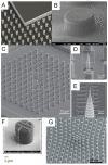
Panel (A) shows a silicon-based superhydrophobic concentrator having at its center a hydrophilic area to collect the concentrated material. Panel (B) reports a scanning electron microscopy (SEM) image of a SU8 pillar of a SHS. Plasma etching was used to create a “dual scale topography” to enhance the superhydrophobic behavior of the surface. Panel (C) (with higher magnification details in (D) and (E)) reports a SEM image of a silicon-made superhydrophobic concentration device having at its center a plasmonic focusing tip to enhance the local electric field for few-molecule Raman signal excitation. A SEM picture of a pillar realized on silicon is shown in (F), which has a dual-electrode sensor fabricated on its top and contacted for electrical measurements. Panel (G) shows a SEM image of an arrangement of SU8-grown pillars, in this case, realized on a silicon nitride membrane for sample optical and X-ray transparency, having a positive pillar density gradient toward the center to force the suspended drop in this position while maintaining the superhydrophobic state. (A) Reproduced with permission from ref. [116]. (B) Reprinted with permission from ref. [87]. (CE) Reprinted with permission from ref. [66]. (F) Reprinted with permission from ref. [67]. (G) Reprinted with permission from ref. [73].
Figure 5
Figure 5
Silicon-based SHSs for material stretching across pillars. Panel (A) shows a SEM picture of a deposition of Deoxyribonucleic acid (DNA) bundles stretched across a silicon-made SHS. Authors demonstrated the possibility to have control on the orientation and vertical position of the created bundles. Panels B,C: side (B) and top (C) view of a silicon-based SHS with DNA bundles stretched across the interpillar gaps. It is then possible to obtain High-Resolution Transmission Electron Microscopy (HRTEM) images of the bundles that show a periodic structure of the filament, which is coherent with known values of DNA helical structure (shown in (D), with magnified view in the inset). Panel (E) displays a SEM view of a microfabricated silicon SHS, perforated to allow TEM analysis of the deposited material. The picture shows the formation of fibrils resulting from the evaporation in the superhydrophobic state of a physiological solution containing Tau441 proteins stretching across the pillars. Elongated holes between the pillars assure complete transparency to the electron beam even upon sample tilting. Scale bar in panel (A) = 5 μm; in (B) and (C) = 1 μm; and in (D) = 20 nm. (A) Adapted from ref. [123]. (BD) Adapted from ref. [69]. (E) Adapted from ref. [154].
Figure 6
Figure 6
SHSs for cells and cellular membranes deposition. (A) Structure of a DRIE-made silicon pillar and (B) experimental realization with a regular arrangement. (C) and (D) show the lateral profiles of two different implementations: in (C), the smooth side surface of the pillar is obtained by using a single etching step; in (D), standard DRIE process with alternation of deposition and etching phases results in the typical saw-teeth profile, an effect usually termed scalloping. This latter lateral profile has been proved to be important to promote adhesion of cells and is preferred for this application. (E) Image of a water drop suspended on an SHS. (F) SEM image that shows the presence of a large neuron (black *) with its multiple neuritic processes (arrows) spreading on top of a flat glial cell monolayer (white *), suspended on a silicon-made SHS identical to that shown in (B). (G,H) SEM tilted views of a silicon-made SHS over which cellular membranes have been suspended and stretched. Scale bars: 10 μm in (B), 5 μm in (C,D,F). (AE) Reprinted with permission from ref. [64]. (F) Adapted from ref. [64]. (G,H) Reprinted with permission from ref. [120].

Similar articles

Cited by

References

    1. Koch K., Bhushan B., Barthlott W. Multifunctional surface structures of plants: An inspiration for biomimetics. Prog. Mater. Sci. 2009;54:137–178. doi: 10.1016/j.pmatsci.2008.07.003. - DOI
    1. Wong T.S., Sun T., Feng L., Aizenberg J. Interfacial materials with special wettability. MRS Bull. 2013;38:366–371. doi: 10.1557/mrs.2013.99. - DOI
    1. Ren T., He J. Substrate-versatile approach to robust antireflective and superhydrophobic coatings with excellent self-cleaning property in varied environments. ACS Appl. Mater. Interfaces. 2017;9:34367–34376. doi: 10.1021/acsami.7b11116. - DOI - PubMed
    1. Blossey R., Scientifique C. 2003_Self-cleaning surfaces–virtual realities_Nature. Nat. Publ. Gr. 2003;2:301–306. - PubMed
    1. Ghasemlou M., Le P.H., Daver F., Murdoch B.J., Ivanova E.P., Adhikari B. Robust and Eco-Friendly Superhydrophobic Starch Nanohybrid Materials with Engineered Lotus Leaf Mimetic Multiscale Hierarchical Structures. ACS Appl. Mater. Interfaces. 2021;13:36558–36573. doi: 10.1021/acsami.1c09959. - DOI - PubMed