

Mechanical/Electrical Characterization of ZnO Nanomaterial Based on AFM/Nanomanipulator Embedded in SEM
- PMID: 33671034
- PMCID: PMC7997223
- DOI: 10.3390/mi12030248
Mechanical/Electrical Characterization of ZnO Nanomaterial Based on AFM/Nanomanipulator Embedded in SEM
Abstract
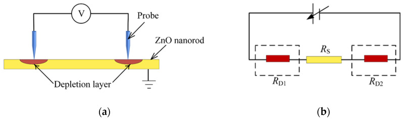
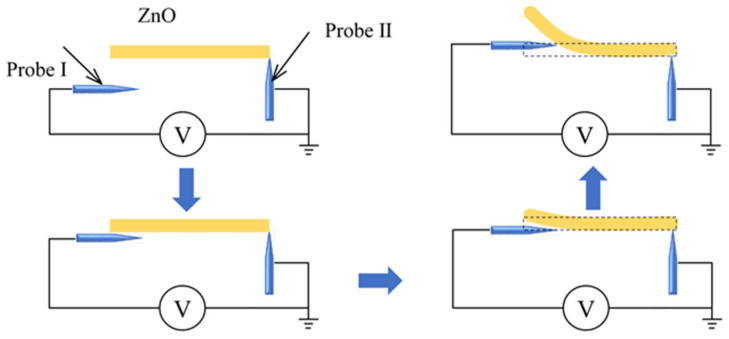
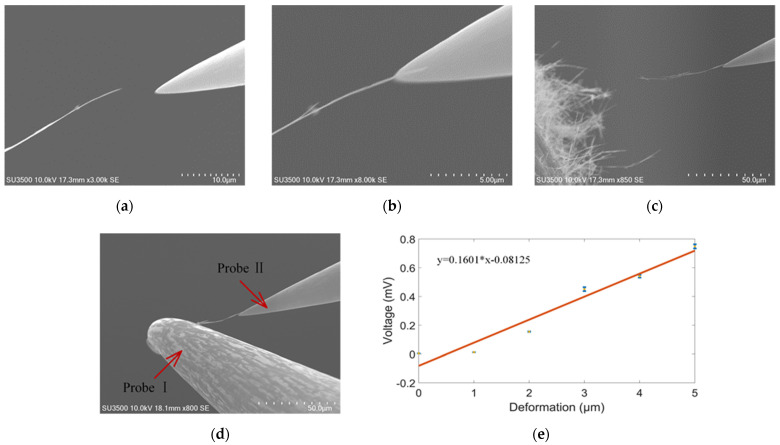
ZnO nanomaterials have been widely used in micro/nano devices and structure due to special mechanical/electrical properties, and its characterization is still deficient and challenging. In this paper, ZnO nanomaterials, including nanorod and nanowire are characterized by atomic force microscope (AFM) and nanomanipulator embedded in scanning electron microscope (SEM) respectively, which can manipulate and observe simultaneously, and is efficient and cost effective. Surface morphology and mechanical properties were observed by AFM. Results showed that the average Young's modulus of ZnO nanorods is 1.40 MPa and the average spring rate is 0.08 N/m. Electrical properties were characterized with nanomanipulator, which showed that the ZnO nanomaterial have cut-off characteristics and good schottky contact with the tungsten probes. A two-probe strategy was proposed for piezoelectric property measurement, which is easy to operate and adaptable to multiple nanomaterials. Experiments showed maximum voltage of a single ZnO nanowire is around 0.74 mV. Experiment criteria for ZnO manipulation and characterization were also studied, such as acceleration voltage, operation duration, sample preparation. Our work provides useful references for nanomaterial characterization and also theoretical basis for nanomaterials application.
Keywords: ZnO; atomic force microscope; mechanical/electrical characterization; nanomanipulator; piezoelectric property.
Conflict of interest statement
The authors declare no conflict of interest.
Figures

Similar articles
-
Synthesis of ZnO Nanorod Film Deposited by Spraying with Application for Flexible Piezoelectric Energy Harvesting Microdevices.Sensors (Basel). 2020 Nov 26;20(23):6759. doi: 10.3390/s20236759. Sensors (Basel). 2020. PMID: 33256037 Free PMC article.
-
Electrical Activity and Extremes of Individual Suspended ZnO Nanowires for 3D Nanoelectronic Applications.ACS Appl Mater Interfaces. 2023 Sep 20;15(37):44433-44443. doi: 10.1021/acsami.3c07418. Epub 2023 Sep 8. ACS Appl Mater Interfaces. 2023. PMID: 37682724
-
Simultaneous acquisition of current and lateral force signals during AFM for characterising the piezoelectric and triboelectric effects of ZnO nanorods.Sci Rep. 2021 Feb 3;11(1):2904. doi: 10.1038/s41598-021-82506-8. Sci Rep. 2021. PMID: 33536507 Free PMC article.
-
Recent Advances on SEM-Based In Situ Multiphysical Characterization of Nanomaterials.Scanning. 2021 Jun 9;2021:4426254. doi: 10.1155/2021/4426254. eCollection 2021. Scanning. 2021. PMID: 34211620 Free PMC article. Review.
-
Profiling to Probing: Atomic force microscopy to characterize nano-engineered implants.Acta Biomater. 2023 Oct 15;170:15-38. doi: 10.1016/j.actbio.2023.08.006. Epub 2023 Aug 9. Acta Biomater. 2023. PMID: 37562516 Review.
Cited by
-
Controllable Melting and Flow of Ag in Self-Formed Amorphous Carbonaceous Shell for Nanointerconnection.Micromachines (Basel). 2022 Jan 29;13(2):213. doi: 10.3390/mi13020213. Micromachines (Basel). 2022. PMID: 35208338 Free PMC article.
References
-
- Zhao X., Yang S., Sun Z., Cui N., Zhao P., Tang Q., Tong Y., Liu Y. Enhancing the intrinsic stretchability of micropatterned gold film by covalent linkage of carbon nanotubes for wearable electronics. ACS Appl. Electron. Mater. 2019;1:1295–1303. doi: 10.1021/acsaelm.9b00243. - DOI
-
- Yamazaki H., Hayashi Y., Masunishi K., Ono K., Ikehashi T. High sensitivity MEMS capacitive hydrogen sensor with inverted T-shaped electrode and ring-shaped palladium alloy for fast response and low power consumption. Micromech. Microeng. 2018;28:094001. doi: 10.1088/1361-6439/aac21d. - DOI
-
- Bandekar G., Rajurkar N.S., Mulla I.S., Mulik U.P., Amalnerkar D.P., Adhyapak P.V. Synthesis, characterization and photocatalytic activity of PVP stabilized ZnO and modified ZnO nanostructures. Appl. Nanosci. 2013;4:199–208. doi: 10.1007/s13204-012-0189-2. - DOI
Grants and funding
LinkOut - more resources
Full Text Sources
Other Literature Sources
Miscellaneous
