Review
. 2019 Dec 16;9(12):1789.
doi: 10.3390/nano9121789.

The Fabrication of Micro/Nano Structures by Laser Machining

Affiliations
Review

The Fabrication of Micro/Nano Structures by Laser Machining

Liangliang Yang et al. Nanomaterials (Basel). .

Abstract

Micro/nano structures have unique optical, electrical, magnetic, and thermal properties. Studies on the preparation of micro/nano structures are of considerable research value and broad development prospects. Several micro/nano structure preparation techniques have already been developed, such as photolithography, electron beam lithography, focused ion beam techniques, nanoimprint techniques. However, the available geometries directly implemented by those means are limited to the 2D mode. Laser machining, a new technology for micro/nano structural preparation, has received great attention in recent years for its wide application to almost all types of materials through a scalable, one-step method, and its unique 3D processing capabilities, high manufacturing resolution and high designability. In addition, micro/nano structures prepared by laser machining have a wide range of applications in photonics, Surface plasma resonance, optoelectronics, biochemical sensing, micro/nanofluidics, photofluidics, biomedical, and associated fields. In this paper, updated achievements of laser-assisted fabrication of micro/nano structures are reviewed and summarized. It focuses on the researchers' findings, and analyzes materials, morphology, possible applications and laser machining of micro/nano structures in detail. Seven kinds of materials are generalized, including metal, organics or polymers, semiconductors, glass, oxides, carbon materials, and piezoelectric materials. In the end, further prospects to the future of laser machining are proposed.

Keywords: application; femtosecond laser; laser machining; material; mental; micro/nano fabrication; micro/nano structures; semiconductor.


Conflict of interest statement

The authors declare no conflict of interest.

Figures

Figure 1
Figure 1
Laser-assisted preparation of metal nanoparticle arrays (a) Scheme of nanoparticle structure fabrication by a combination of the nanosphere lithography and laser-induced transfer. (b) Dark-field microscope image of arrays of gold nanoparticles fabricated by single laser pulses on a receiver substrate. Laser fluence is of 0.06 J/cm2. (c) Top-view scanning electron microscope (SEM) image of nanoparticle arrays prepared by a single laser pulse. (d) Schematic process of the Au nanoparticle-decorated nanorod (NPDN) substrate fabrication. SEM images of Au nanoparticles (NPs) formed on three categories of substrates coated with 10 nm Au films and annealing: (e) flat Si, (f) ripple, and (g) nanorod substrates. Scale bars indicate 500 nm. (ac) reproduced with permission from [62], ACS, 2011; (dg) reproduced with permission from [63], ACS, 2018.
Figure 2
Figure 2
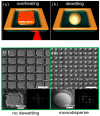
Metal nanoparticles fabricated by laser dewetting (a,b) Schematic diagram of a femtosecond laser cutting a patch on an Au film on a dielectric substrate to form a single nanoparticle; (c) SEM image before laser dewetting; (d) SEM image of an Au nanoparticle array made of a 30 nm film on a SiO2 substrate at a fluence of 40 mJ/cm2. The lower right insets: Fourier spectra of the SEM images. The lower left insets: enlarged SEM images of typical nanoparticles from the arrays. (ad) reproduced with permission from [67], Wiley, 2016.
Figure 3
Figure 3
The preparation of high-resolution nanowires by Space-modulated femtosecond laser beam. (a) Schematic diagram of the experimental setup. (b1b5) SEM images of the short nanowires formed between the two spots with increasing pulse energy. (c,d) Short nanowires formed using thin gold film with (c) 20 nm and (d) 10 nm thickness (both consisting of 3 nm Cr as the adhesion layer). The scale bar is 1 µm. (e) The cross-section of the nanowires shown in (b) measured by atomic force microscopy (AFM). (f) Section area decreased and height increased with the pulse energy. (g) The cross-section of the minimum nanowires using different film thicknesses was measured by AFM. (ag) reproduced with permission from [74], Wiley, 2015.
Figure 4
Figure 4
The preparation of high-resolution patterns by femtosecond laser selective nanoparticles (NPs) sintering (FLSNS). (a) Variation of the line width depending on the scanning speed at 150, 200, 300, and 400 mW laser powers. The inset shows a scanning electron microscopy (SEM) image of the fabricated metal line at 150 mW and 400 μm s−1. (b) SEM images of the fabricated 2D metal clover patterns. (a,b) reproduced with permission from [86], Wiley, 2011.
Figure 5
Figure 5
The laser-assisted fabrication of 3D structures. (a) Fabrication scheme of 3D metallic bichiral crystals through direct laser writing and electroless silver plating. (b) SEM images of a bichiral crystal with right-handed corners and righthanded helices after electroless silver plating. (a,b) reproduced with permission from [95], Wiley, 2011.
Figure 6
Figure 6
Diagram of 3D laser direct writing technology to prepare 3D micro/nano structure. (a) Schematic diagram of the apparatus used for 3D laser direct-write. (b) Conceptual diagrams illustrating the basic steps for the non-contact 3D laser direct write process. (c) A high aspect ratio micro pyramid. (d) SEM image of an interconnect bonding Cu electrodes on Si. (ad) reproduced with permission from [101], Wiley, 2010.
Figure 7
Figure 7
Diagram of 3D micro/nano structures by laser machining. (a) Schematic of the construction of the samples used during laser machining. (b) SEM images of the Ag deposits resulting from illumination from the glass with 4.25 mW of 632.8 nm laser light focused with a 50× objective lens to a ~1 µm spot after 10 s of illumination and the yellow dotted line presents that the width of the silver deposit increases approximately proportionally with the radial distance from the center of the deposit. (c) Schematic diagram of asymmetric metal dielectric (Au/Si) nanoparticles prepared by photolithography of femtosecond laser melting. (d) The SEM images correspond to the typical structures in the following modification regimes: Au nanodisc deformation, transformation to Au nanospheres, Si nanocone melting, and damage of the nanodimer. (e) Molecular dynamics simulation of the Au nanoparticle reshaping. (a,b) reproduced with permission from [104], ACS, 2010; (ce) reproduced with permission from [105], Wiley, 2016.
Figure 8
Figure 8
Diagram of large area micro/nano structure prepared by laser machining. (a) Schematic diagram of an experimental setup for 3D chiral microstructure in an isotropic material based on spatial light modulator (SLM). (b) SEM images of chiral microstructures with three spiral lobes achieved for different values of laser power and exposure time. (Scale bar, 5 μm). (c) Quantitative study of the diameter of the chiral microstructure as a function of exposure time and power. (d) Schematic of heat-induced shrinkage of shape-memory polymer (SMP) film by a hot air gun. Inset: pictures of polystyrene film before and after heating. The red semicircle indicates the laser scanning path. (e,f) SEM of polystyrene film after laser machining. (ac) reproduced with permission from [113], Nature, 2017; and (df) reproduced with permission from [114], Wiley, 2018.
Figure 9
Figure 9
Three-dimensional photonic crystal structures fabricated by the two-photon polymerization (TPP) technique. (a,b) reproduced with permission from [118], ACS, 2008.
Figure 10
Figure 10
Diagram of 2D/3D polymer structures by two-photon polymerization lithography (a) Fabricative procedures of remotely controllable micronanomachines. (b1b4) SEM images of the micro-turbine. (a,b) reproduced with permission from [121], Wiley, 2010.
Figure 11
Figure 11
Illustration of 2D/3D polymer structures by two-photon polymerization lithography (a) Diagram of the fabrication process of high-performance asymmetric polymer microcavities on a cover glass. (b) SEM image of asymmetric polymer microcavities. (c) Experimental procedure in preparing multiwalled carbon nanotube-thiol-acrylate (MTA) composite resins. (d) Experimental setup of two-photon polymerization (TPP) fabrication. (e) Physical map of a bent polyethylene terephthalate (PET) substrate. (fj) SEM micrographs of various functional micro/nano structures. The laser power and scanning speed used in the TPP fabrication were 15 mW and 0.5 mm s−1, respectively. (a,b) reproduced with permission from [129], AIP, 2013; and (cj) reproduced with permission from [130], Wiley, 2016.
Figure 12
Figure 12
Diagram of extended periodic microstructure of a two-photon direct laser writing (DLW). (a) Pinciple of two-photon lithography. (b) SEM images of spiral structures. (c) A detailed SEM view of the individual spirals. (ac) reproduced with permission from [134], Wiley, 2005.
Figure 13
Figure 13
Diagram of 3D composite polymer scaffolds by DLW. (a) 3D frameworks are polymerized and fabricated. (b) Frameworks are then cast with the photoresist Ormocomp and cubes (one cube is highlighted in red) are precisely attached to the polyethylene glycol diacrylate (PEG-DA) beams in a second DLW step. (c) Higher magnification image of an Ormocomp cube (highlighted in red). (ac) reproduced with permission from [137], Wiley, 2011.
Figure 14
Figure 14
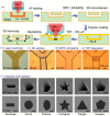
3D polymer micro/nano structures by hybrid femtosecond laser micromachining. (a) Schematic illustration of the fabrication procedure for a 3D ship-in-a-bottle biochip by hybrid fs laser micro processing. 3D Y-shaped microchannel after laser scanning and the first annealing (b), hydrofluoric acid (HF) etching (c), second annealing (d) and 3D integration of polymer microstructure by TPP (e). SEM images of controllable cross sections of the 3D micro-channels. (af) reproduced with permission from [141], Wiley, 2014.
Figure 15
Figure 15
Diagram of 3D cell culture scaffolds by DLW. (a) Schematic diagram: direct laser writing (DLW) was applied to fabricate non-cytotoxic 3D scaffolds on porous membranes. (b) SEM side view and top view images of a 3D scaffold with a mesh size of 10 μm resting on a membrane with a pore diameter of 3 μm. (a,b) reproduced with permission from [142], Elsevier, 2013.
Figure 16
Figure 16
Three-dimensional microstructured mechanical metamaterial by DLW. (a) Diagram of conventional three-dimensional direct laser writing lithography. (b) Diagram of a new immersive 3D-DLW method. Sample height is no longer fundamentally restricted. (c) Oblique-view electron microscopy images of selected fabricated mechanical metamaterials on glass substrates. (ac) reproduced with permission from [145], Wiley, 2012.
Figure 17
Figure 17
Diagram of polymer nanopillars (NP) using 3D direct laser writing. (a) View of a full 250 × 250 µm2 NP array and an inset of a tilted SEM about the edge of an array. (bg) Different polymeric NP center-to-center spacings: 1.5 µm (b), 2 µm (c), 3 µm (d), 4 µm (e), 6 µm (f), and 12 µm (g). All NPs here have length 3 µm. (ag) reproduced with permission from [152], Springer Nature, 2017.
Figure 18
Figure 18
Diagram of micro/nano-scale combined layered structures by laser swelling technology. (ad) Schematic diagram of the fabrication process: (a) Swelling polymer and UV curable prepolymer are fabricated on a glass substrate. (b) Secondary pillar structures are prepared by nanoimprinting. (c) Laser beam is irradiated on the swelling polymer to form a primary structure from the side of substrate. (d) Formation of fully covering hierarchical micro/nano structures. (e,f) SEM images of various hierarchical structures. (af) reproduced with permission from [162], Wiley, 2014.
Figure 19
Figure 19
Laser-induced periodic surface structure by continuous wave (CW) laser. (a) schematics of two CW laser system. (b) SEM image of laser induced periodic surface structures (LIPSS). The laser irradiates the target at a scanning speed of 300 m/min. The inset is an enlarged view. (a,b) reproduced with permission from [171], Elsevier, 2013.
Figure 20
Figure 20
Diagram of anti-reflective microstructures on Si surfaces by DLW. (a) Schematic of fiber laser ablation for black Si surface fabrication. (b) Image of the textured black Si surface. (c) SEM image and (d) 3D surface profile. (ad) reproduced with permission from [184], Springer Nature, 2014.
Figure 21
Figure 21
Diagram of 3D photonic crystals by DLW. (a) Schematic of the woodpile structure. (b,c) SEM images of a methylsilsesquioxane (MSQ) woodpile structure. The spacing between the lines was 4 μm and the lateral size of the photonic crystals was about 116 × 116 μm. (a,c) reproduced with permission from [196], Wiley, 2008.
Figure 22
Figure 22
Diagram of silicon micro/nano structures of controlled size and shape by chemical translation assisted femtosecond laser single pulse irradiation. (ac) Schematic diagram of the experimental process. (df) SEM images of a Si wafer after laser irradiation. (gi) SEM images of a Si wafer after KOH etching for 90 s. Right upper insets are the magnified SEM images of single Si structures; Right lower insets are the AFM images of Si structures. (jl) AFM images of single Si fabricated structure corresponding to (gi). (al) reproduced with permission from [205], AIP, 2017.
Figure 23
Figure 23
Diagram of silicon micro/nano structures fabricated by dry etching assisted femtosecond laser machining. (a) Diagram of the fabrication of silicon structures using dry etching assisted femtosecond laser machining (DE-FsLM). The inset is the SEM image of the prepared silicon concave structures. (b) Diagram of the cross-sectional profiles of the concave structures to present the etching process. (a,b) reproduced with permission from [211], Wiley, 2017.
Figure 24
Figure 24
Diagram of inverted pyramidal pits (IPP) by laser machining. (ag) Schematic view of the fabricate on process of 3D container which is composed of IPP array with nano-openings. (h,i) SEM and AFM images of the 3D container, respectively. (j) SEM image of the 3D container. (k) An detailed image of 3D containers with critical size parameters. (ak) reproduced with permission from [217], Elsevier, 2016.
Figure 25
Figure 25
Diagram of the direct laser writing of a 3D photonic crystal. (a) The three fabrication steps of 3D photonic crystal by DLW. (a) Woodpile with rod distance 2 μm to illustrate the construction principle of the rods; Inset image shows Each rod is fabricated from eight parallel subrods to yield a rod aspect ratio of almost 1.0. (ce) SEM images of As2S3 woodpiles. (ae) reproduced with permission from [223], Wiley, 2006.
Figure 26
Figure 26
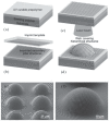
Diagram of 3D micro/nano structures by laser machining. (a) Schematic diagrams of the preparation process and the laser exposure methods. (b) Poly (dimethylsiloxane) (PDMS) replicas of the microwells of conical microstructures (c) magnified observations of (b). (ac) reproduced with permission from [243], Elsevier, 2013.
Figure 27
Figure 27
Diagram of nanodot arrays by pulsed laser deposition. (a) Procedure for the nanodot array fabrication. (b) AFM image of an as-deposited CoFe2O4 (CFO) nanodot array. (c) CFO nanodot array together with a partially removed anodic aluminum oxide (AAO) mask. (ac) reproduced with permission from [254], Wiley, 2009.
Figure 28
Figure 28
Diagram of the application of laser scribing graphene. (a). Diagram of the main fabrication processing steps of the laser scribing graphene-resistive random access memory (LSG-ReRAM). (b) Top view SEM image ofthe LSG-ReRAM in false color. (a,b) reproduced with permission from [284], ACS, 2014.
Figure 29
Figure 29
Diagram of single-walled carbon nanotubes (CNTs) 3D nanostructures fabricated by DLW. (a) Schematic showing 3D microfabrication of single-walled CNTs (SWCNT)/polymer composites based on TPP lithography. (b,c) SEM images of a 375 nm wide, 10 µm long nanowire, suspended between two microboxes. (d) SEM image of a cross-section of the nanowire. (ad) reproduced with permission from [288], Wiley, 2014.
Figure 30
Figure 30
Diagram of ZnO nanostructures fabricated by CO2 lasers. (ag) SEM images of the ZnO nanostructures with various morphologies. (ag) reproduced with permission from [314], Elsevier, 2010.

Similar articles

Cited by

References

    1. Zang X., Zhou Q., Chang J., Liu Y., Lin L. Graphene and carbon nanotube (CNT) in MEMS/NEMS applications. Microelectron. Eng. 2015;132:192–206. doi: 10.1016/j.mee.2014.10.023. - DOI
    1. Ma R., Sasaki T. Nanosheets of oxides and hydroxides: Ultimate 2D charge-bearing functional crystallites. Adv. Mater. 2010;22:5082–5104. doi: 10.1002/adma.201001722. - DOI - PubMed
    1. Archana P., Jose R., Vijila C., Ramakrishna S.J. Improved electron diffusion coefficient in electrospun TiO2 nanowires. J. Phys. Chem. C. 2009;113:21538–21542. doi: 10.1021/jp908238q. - DOI
    1. Bhushan B., Jung Y.C. Natural and biomimetic artificial surfaces for superhydrophobicity, self-cleaning, low adhesion, and drag reduction. Prog. Mater. Sci. 2011;56:1–108. doi: 10.1016/j.pmatsci.2010.04.003. - DOI
    1. Klaus-Joerger T., Joerger R., Olsson E., Granqvist C.G.J. Bacteria as workers in the living factory: metal-accumulating bacteria and their potential for materials science. TRENDS Biotechnol. 2001;19:15–20. doi: 10.1016/S0167-7799(00)01514-6. - DOI - PubMed

LinkOut - more resources