

doi: 10.1021/acs.chemmater.6b04469.
Epub 2017 Jan 23.
Area-Selective Atomic Layer Deposition of In2O3:H Using a μ-Plasma Printer for Local Area Activation
Affiliations
- PMID: 28405058
- PMCID: PMC5384477
- DOI: 10.1021/acs.chemmater.6b04469
Item in Clipboard
Area-Selective Atomic Layer Deposition of In2O3:H Using a μ-Plasma Printer for Local Area Activation
Chem Mater.
.
No abstract available
Conflict of interest statement
The authors declare no competing financial interest.
Figures
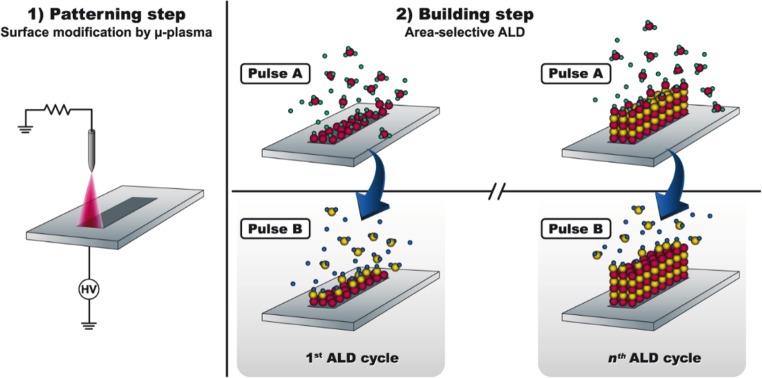
Schematic representation of the area-selective ALD process
of In2O3:H on H-terminated silicon materials.
In the
first step (1), microscale patterns are defined by activating the
surface with a μ-plasma operated in air or O2. In
the second step (2), the In2O3:H is deposited
selectively on the activated areas in a building step. The ALD process
consists of two alternating half reactions: InCp precursor dosing
in pulse A and a mixture of O2 and H2O dosing
in pulse B. Note that in the case that conductive substrates are used,
a thin dielectric membrane (Al2O3) is positioned
between the needles and the substrate, as shown in Figure S1a .
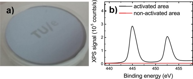
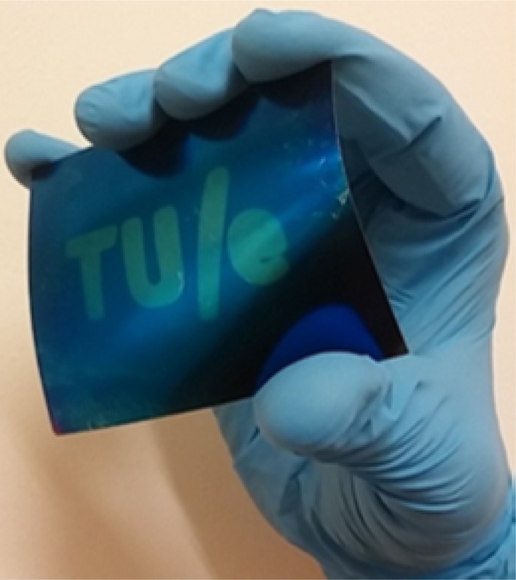
(a) Photograph
of a 4-in. Si(100) wafer covered with 10 nm of a-Si:H
with the letters “TU/e” prepared using the direct-write ALD process of In2O3:H. The number of ALD
cycles was 400 and the thickness of the In2O3:H was ∼35 nm. (b) XPS signals for the In 3d5/2 and In 3d3/2 binding energy measured for two distinctive
points inside (black) and outside (red) the patterned area.
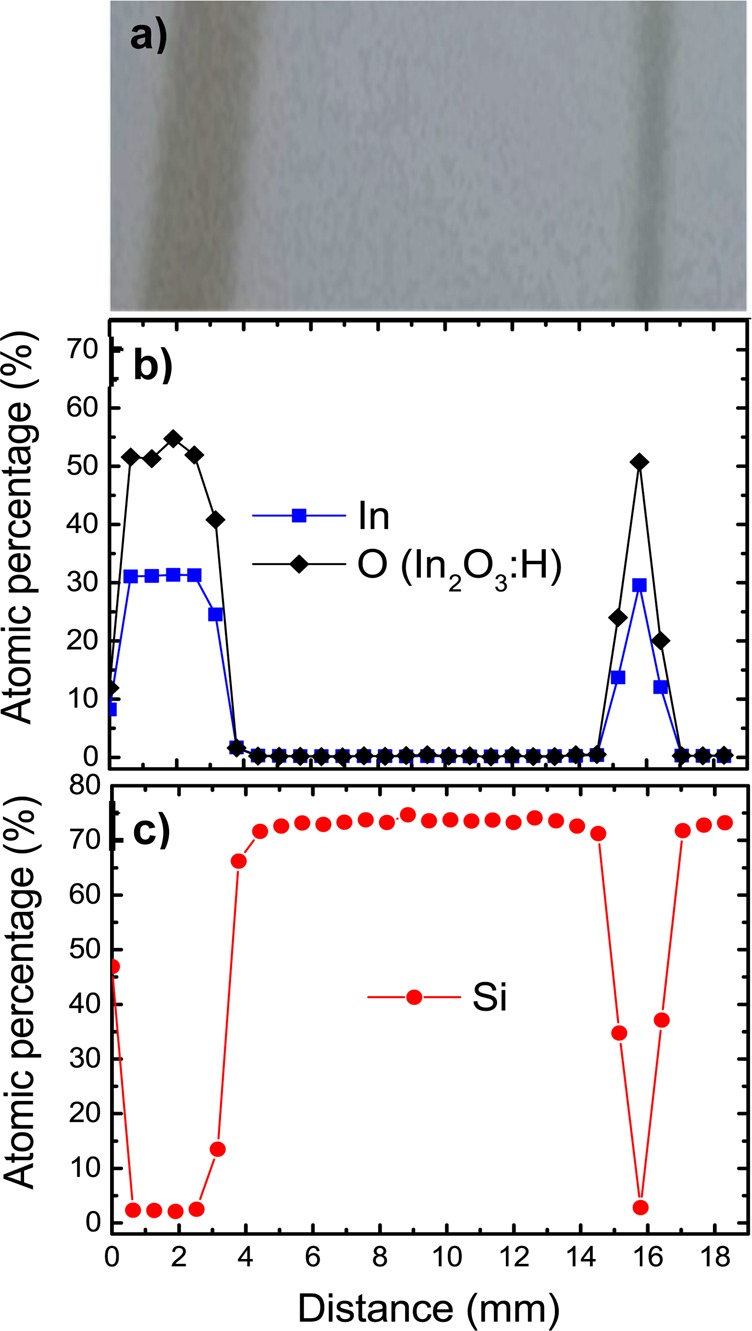
(a) Photograph of In2O3:H lines
being 3.0
and 0.8 mm wide as prepared by the direct-write ALD process with 400
cycles. XPS line scans for the patterns depicted in (a) showing the
atomic percentages related to (b) In2O3 (In
3d5/2 and O 1s) and (c) the Si substrate (Si 2p).
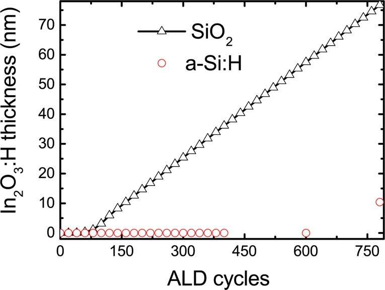
Film thickness measured by in situ SE as a function
of the In2O3:H ALD cycles on SiO2 (open triangles)
and on a-Si:H (open circles). Ex situ SE measurements were taken only
for 600 and 780 ALD cycles on a-Si:H. Above 600 ALD cycles the selectivity
of the process appears to degrade.
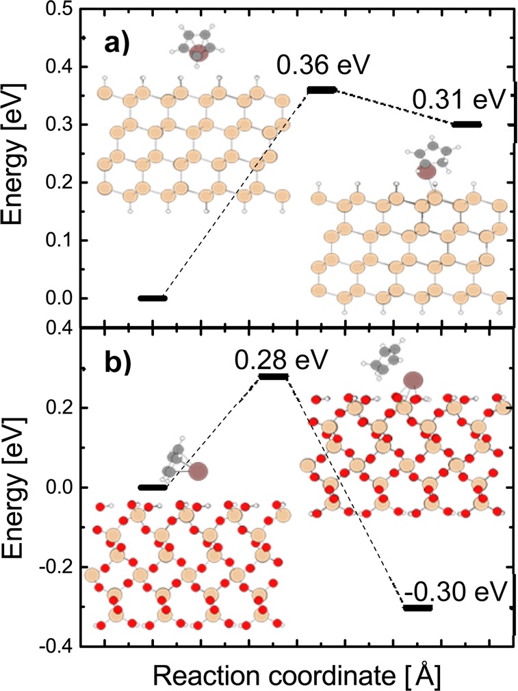
Energy profiles
computed by DFT method (PBE-D3) for the chemisorption
of InCp on (a) hydrogenated silicon (Si–H termination) and
(b) on hydroxylated silicon oxide (Si–OH termination).
Pattern
prepared by direct-write ALD of a 35 nm
thick In2O3:H film on a flexible stainless steel
foil covered with 20 nm of a-Si:H. This serves as a first demonstrator
of the capability of the direct-write ALD process
for large-area and flexible electronics.
Similar articles
-
From the Bottom-Up: Toward Area-Selective Atomic Layer Deposition with High Selectivity.Chem Mater. 2019 Jan 8;31(1):2-12. doi: 10.1021/acs.chemmater.8b03454. Epub 2018 Dec 19. Chem Mater. 2019. PMID: 30774194 Free PMC article. Review.
-
Electron Scattering and Doping Mechanisms in Solid-Phase-Crystallized In2O3:H Prepared by Atomic Layer Deposition.ACS Appl Mater Interfaces. 2015 Aug 5;7(30):16723-9. doi: 10.1021/acsami.5b04420. Epub 2015 Jul 23. ACS Appl Mater Interfaces. 2015. PMID: 26168056
-
Low-Temperature Growth of Indium Oxide Thin Film by Plasma-Enhanced Atomic Layer Deposition Using Liquid Dimethyl(N-ethoxy-2,2-dimethylpropanamido)indium for High-Mobility Thin Film Transistor Application.ACS Appl Mater Interfaces. 2016 Oct 12;8(40):26924-26931. doi: 10.1021/acsami.6b07332. Epub 2016 Sep 27. ACS Appl Mater Interfaces. 2016. PMID: 27673338
-
High-Performance On-Chip Supercapacitors Based on Mesoporous Silicon Coated with Ultrathin Atomic Layer-Deposited In2O3 Films.ACS Appl Mater Interfaces. 2019 Jan 9;11(1):747-752. doi: 10.1021/acsami.8b17093. Epub 2018 Dec 21. ACS Appl Mater Interfaces. 2019. PMID: 30525419
-
Indium-tris-guanidinates: a promising class of precursors for water assisted atomic layer deposition of In2O3 thin films.Dalton Trans. 2014 Jan 21;43(3):937-40. doi: 10.1039/c3dt52746h. Epub 2013 Nov 22. Dalton Trans. 2014. PMID: 24264622
Cited by
-
From the Bottom-Up: Toward Area-Selective Atomic Layer Deposition with High Selectivity.Chem Mater. 2019 Jan 8;31(1):2-12. doi: 10.1021/acs.chemmater.8b03454. Epub 2018 Dec 19. Chem Mater. 2019. PMID: 30774194 Free PMC article. Review.
-
Area-Selective Atomic Layer Deposition of SiO2 Using Acetylacetone as a Chemoselective Inhibitor in an ABC-Type Cycle.ACS Nano. 2017 Sep 26;11(9):9303-9311. doi: 10.1021/acsnano.7b04701. Epub 2017 Sep 7. ACS Nano. 2017. PMID: 28850774 Free PMC article.
-
Atmospheric-pressure atomic layer deposition: recent applications and new emerging applications in high-porosity/3D materials.Dalton Trans. 2023 Aug 1;52(30):10254-10277. doi: 10.1039/d3dt01204b. Dalton Trans. 2023. PMID: 37376785 Free PMC article. Review.
-
Inherently Area-Selective Atomic Layer Deposition of Manganese Oxide through Electronegativity-Induced Adsorption.Molecules. 2021 May 20;26(10):3056. doi: 10.3390/molecules26103056. Molecules. 2021. PMID: 34065464 Free PMC article.
-
Relation between Reactive Surface Sites and Precursor Choice for Area-Selective Atomic Layer Deposition Using Small Molecule Inhibitors.J Phys Chem C Nanomater Interfaces. 2022 Mar 17;126(10):4845-4853. doi: 10.1021/acs.jpcc.1c10816. Epub 2022 Mar 8. J Phys Chem C Nanomater Interfaces. 2022. PMID: 35330759 Free PMC article.
References
-
- Hua Y.; King W. P.; Henderson C. L. Nanopatterning Materials Using Area Selective Atomic Layer Deposition in Conjunction with Thermochemical Surface Modification via Heated AFM Cantilever Probe Lithography. Microelectron. Eng. 2008, 85, 934–936. 10.1016/j.mee.2008.01.105. - DOI
-
- Kim W.; Lee H.; Heo K.; Lee K.; Chung T.; Kim G.; Hong S.; Heo J.; Kim H. Atomic Layer Deposition of Ni Thin Films and Application to Area-Selective Deposition. J. Electrochem. Soc. 2011, 158, D1–D5. 10.1149/1.3504196. - DOI
-
- Sinha A.; Hess D. W.; Henderson C. L. Area-Selective ALD of Titanium Dioxide Using Lithographically Defined Poly(methyl Methacrylate) Films. J. Electrochem. Soc. 2006, 153, G465–G469. 10.1149/1.2184068. - DOI
LinkOut - more resources
Full Text Sources
Other Literature Sources
Research Materials